In all SSDs there is a central chip that is responsible for communicating the NVMe chips with the rest of the PC components, this is the flash controller that is found in each SSD unit, be it an M.2 unit, an SSD disk in 2.5-inch form factor or an external SSD. But how does this piece of hardware work? We explain it to you.
Flash memory is what we call non-volatile RAM or NVRAM, which is why access to this type of memory is done with a very similar interface, if not almost the same as a conventional memory interface. However, due to the nature and location of NVMe-type NAND Flash memory in SSD hardware, its operation is totally different from interfaces with conventional RAM.
What is a flash controller?
A flash controller is the central chip found in every SSD drive, which has to perform a series of functions that are essential for its operation. These are addressing and copying data from SSD flash memory to system RAM or VRAM. Below we describe the reason and how these two processes work and how the flash controller performs them.

To understand the usefulness of the flash controller in the SSD, it is best to make a simile in which we have two post offices, a state one that has all the addresses of the towns in the country but not in a conventional way. To understand it better, think that each address in our example is not a street with a number, but a PO box or, in other words, a number. And what about the second post office? Well, this works at the scale of a much smaller location, such as a province or a small town.
Since each office is going to assign all the addresses from the first to the last according to the number of addresses it has available, then we find that the numbering of each address assigned by each of the post offices will not correspond to each other. Well, the first post office is the set of memory management units or MMUs that generate the virtual addresses to access the data in physical memory, but the CPU has to have a way to access beyond the RAM and therefore its addressing not only includes all the memory addresses that are in the system RAM but also beyond.
On a physical level, both traditional and non-volatile RAM, which is what we know as flash memory, have different addressing because their interface begins to count on itself and not globally. Hence one of the tasks of the Flash controller is the transfer of memory addresses so that the CPU or any other processor can access it.
Address translation in FLASH
Every flash controller has a RAM memory allocated, except for DRAM-Less where it uses the system RAM with the added latency and loss of performance that this entails. But, contrary to what we can conclude with the naked eye, this memory not only serves as an intermediate data buffer, but is also used for the transfer of addresses.

That is, the RAM memory assigned to the flash controller stores the addresses sent by the CPU, the transfer table and through a simple operation generates the physical memory addresses that allow it to access the data inside the NVMe chips composed of NAND Flash cells, either to read or write on them. And it must be taken into account that this table will get bigger and bigger the more memory the SSD has inside, hence the need for a conventional RAM memory chip.
We can see this for example in the integrated SSD unit of PlayStation 5, where we can see a small memory chip accompanying the NVMe chips, which is common in the vast majority of SSD units, except, as we have mentioned before, we’re talking about a DRAM-Less SSD drive.
Copying data from Flash to RAM or VRAM
Flash memory is better than a conventional hard disk by not inheriting the access problems of classic disk drives. Like its high transfer speed. Despite this advantage over HDDs, it is not an ideal memory so that the CPU can operate with it directly, much less a GPU. If for the classic DDR memories with a higher bandwidth we need the use of caches to alleviate the lack of speed of this, in the case of flash memories this is worse.

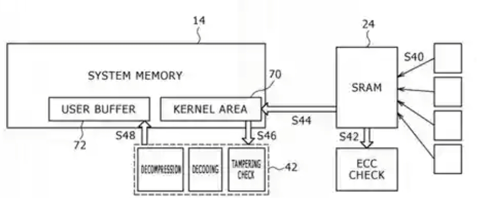
That is why the flash controller needs to copy the data to RAM so that the CPU can access it, but there is an input problem, for security reasons the RAM is divided into two different spaces. One in which applications can access and another that is exclusively accessed by the operating system and where programs cannot access. Under this premise, how does the flash controller know where to copy the data?
Well, a part of the RAM is taken as an intermediate buffer and the data is copied there. It is the CPU of the system itself, if there is no accelerator in charge of this task, the one that would be in charge of checking the data in the buffer and copying it to the corresponding part of the RAM.
Regarding the VRAM, depending on what type of GPU and API we are using, in a GPU with full support with DX12 Ultimate the GPU itself is the one that can take the data from the SSD, in one without said support it requires the participation of the CPU, which is a double job as you then have to copy them from RAM to VRAM by making calls to the CPU and GPU data copy mechanisms.
